- 您现在的位置:买卖IC网 > Sheet目录1993 > DS1302SN-16 (Maxim Integrated Products)IC TIMEKEEPER T-CHRG IND 16-SOIC
AVAILABLE
Functional Diagrams
Pin Configurations appear at end of data sheet.
Functional Diagrams continued at end of data sheet.
UCSP is a trademark of Maxim Integrated Products, Inc.
For pricing, delivery, and ordering information, please contact Maxim Direct
at 1-888-629-4642, or visit Maxim’s website at www.maximintegrated.com.
DS1302
Trickle-Charge Timekeeping Chip
REV: 120208
FEATURES
Real-Time Clock Counts Seconds, Minutes,
Hours, Date of the Month, Month, Day of the
Week, and Year with Leap-Year
Compensation Valid Up to 2100
31 x 8 Battery-Backed General-Purpose RAM
Serial I/O for Minimum Pin Count
2.0V to 5.5V Full Operation
Uses Less than 300nA at 2.0V
Single-Byte or Multiple-Byte (Burst Mode)
Data Transfer for Read or Write of Clock or
RAM Data
8-Pin DIP or Optional 8-Pin SO for Surface
Mount
Simple 3-Wire Interface
TTL-Compatible (VCC = 5V)
Optional Industrial Temperature Range:
-40°C to +85°C
DS1202 Compatible
Underwriters Laboratories (UL)
Recognized
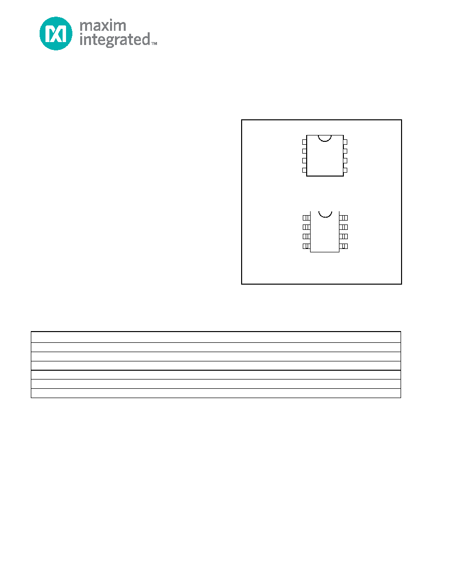
PIN CONFIGURATIONS
ORDERING INFORMATION
PART
TEMP RANGE
PIN-PACKAGE
TOP MARK*
DS1302+
0°C to +70°C
8 PDIP (300 mils)
DS1302
DS1302N+
-40°C to +85°C
8 PDIP (300 mils)
DS1302
DS1302S+
0°C to +70°C
8 SO (208 mils)
DS1302S
DS1302SN+
-40°C to +85°C
8 SO (208 mils)
DS1302S
DS1302Z+
0°C to +70°C
8 SO (150 mils)
DS1302Z
DS1302ZN+
-40°C to +85°C
8 SO (150 mils)
DS1302ZN
+Denotes a lead-free/RoHS-compliant package.
*An N anywhere on the top mark indicates an industrial temperature grade device. A + anywhere on the top mark indicates a lead-free device.
UL is a registered trademark of Underwriters Laboratories, Inc.
VCC1
SCLK
I/O
CE
VCC2
X1
X2
GND
8
7
6
5
1
2
3
4
DIP (300mils)
DS130
2
VCC2
X1
X2
GND
VCC1
SCLK
I/O
CE
8
7
6
5
1
2
3
4
SO (208 mils/150 mils)
DS1302
TOP VIEW
发布紧急采购,3分钟左右您将得到回复。
相关PDF资料
DS1305E/T&R
IC RTC SERIAL ALARM 20-TSSOP
DS1306EN/T&R
IC RTC SERIAL ALARM IND 20-TSSOP
DS1307N
IC RTC SERIAL 512K IND 8-DIP
DS1308U-3+
IC RTC 56BYTE NVRAM I2C 8UMAX
DS1315EN-5/T&R
IC TIME CHIP PHANTOM 20-TSSOP
DS1318E+
IC COUNTER ELAPSED TIME 24-TSSOP
DS1337S+C01
IC RTC SERIAL 2WIRE LP 8-SOIC
DS1338C-33#T&R
IC RTC 56BYTE NV SRAM 16SOIC
相关代理商/技术参数
DS1302SN-16/T&R
制造商:Maxim Integrated Products 功能描述:REAL TIME CLOCK SERL 31BYTE 16SOIC - Tape and Reel 制造商:Maxim Integrated Products 功能描述:IC TIMEKEEPER T-CHRG IND 16-SOIC 制造商:Maxim Integrated Products 功能描述:Real Time Clock Trickle-Charge Timekeeping Chip
DS1302SN-16/T&R
功能描述:实时时钟 Trickle-Charge Timekeeping Chip RoHS:否 制造商:Microchip Technology 功能:Clock, Calendar. Alarm RTC 总线接口:I2C 日期格式:DW:DM:M:Y 时间格式:HH:MM:SS RTC 存储容量:64 B 电源电压-最大:5.5 V 电源电压-最小:1.8 V 最大工作温度:+ 85 C 最小工作温度: 安装风格:Through Hole 封装 / 箱体:PDIP-8 封装:Tube
DS1302SNT&R
制造商:Maxim Integrated Products 功能描述:REAL TIME CLOCK SERL 31BYTE 8SOIC - Tape and Reel
DS1302Z
功能描述:实时时钟 Trickle-Charge Timekeeping Chip RoHS:否 制造商:Microchip Technology 功能:Clock, Calendar. Alarm RTC 总线接口:I2C 日期格式:DW:DM:M:Y 时间格式:HH:MM:SS RTC 存储容量:64 B 电源电压-最大:5.5 V 电源电压-最小:1.8 V 最大工作温度:+ 85 C 最小工作温度: 安装风格:Through Hole 封装 / 箱体:PDIP-8 封装:Tube
DS1302Z/T&R
制造商:Maxim Integrated Products 功能描述:IC TIMEKEEPER T-CHARGE 8-SOIC 制造商:Maxim Integrated Products 功能描述:IC RTC YY-MM-DD 31 X 8 SOIC-8 制造商:Maxim Integrated Products 功能描述:IC, RTC, YY-MM-DD, 31 X 8, SOIC-8
DS1302Z/T&R+
制造商:Maxim Integrated Products 功能描述:REAL TIME CLOCK SERL 31BYTE 8SOIC - Tape and Reel
DS1302Z/T&R
功能描述:实时时钟 Trickle-Charge Timekeeping Chip RoHS:否 制造商:Microchip Technology 功能:Clock, Calendar. Alarm RTC 总线接口:I2C 日期格式:DW:DM:M:Y 时间格式:HH:MM:SS RTC 存储容量:64 B 电源电压-最大:5.5 V 电源电压-最小:1.8 V 最大工作温度:+ 85 C 最小工作温度: 安装风格:Through Hole 封装 / 箱体:PDIP-8 封装:Tube
DS1302Z/T&R/C06
功能描述:实时时钟 Trickle-Charge Timekeeping Chip RoHS:否 制造商:Microchip Technology 功能:Clock, Calendar. Alarm RTC 总线接口:I2C 日期格式:DW:DM:M:Y 时间格式:HH:MM:SS RTC 存储容量:64 B 电源电压-最大:5.5 V 电源电压-最小:1.8 V 最大工作温度:+ 85 C 最小工作温度: 安装风格:Through Hole 封装 / 箱体:PDIP-8 封装:Tube